

- Home
- Companies
- Winovus Pte Ltd.
- Products
- Winovus - Nanoinjection Molding ...
Winovus - Nanoinjection Molding Technology
Injection molding and 3D printing are the standard production technology for plastic parts. However, they are limited to fabricating features and patterns of less than 20 microns in resolution.
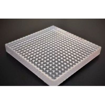
Our nanoinjection molding technology can achieve a pattern structure of size smaller than 20 microns and is suitable for mass production. Nanoinjection molding technology combines elements of nanoimprinting with injection molding, to create three-dimensional (3D) free-form plastic products, with a micro and nanometer-scaled patterned surface.
Nanoinjection molding allows the creation of micro and nanometer-scale structures of resolutions as high as 0.5 micron to be molded directly. As a result, additional surface optical and mechanical functionalities can be added to the plastic molded products, for lab-on-a-chip and optical components applications.
The pivotal element to nanoinjection molding is the mold inserts. We use lithography and electroforming technology to create nanometer-scale patterned inserts. These sub-micron high–resolution inserts are made of hybrid nickel-steel and nickel shim. The polymer material used in nanoinjection molding are PC, PMMA COC/COP, PS or ABS, depending on the application.
Winovus is a pioneer leader in nanoinjection molding. Our state-of-the-art molding facilities are equipped with automated handling robotics, complete with in-situ and ex-situ inspection and quality control. Nanoinjection molding enables new product innovation in the consumer wearable and biomedical sector. It can value adds an existing product by imparting surface functionalities.
Integrating multiple functionalities on molded plastic. Plastic is relatively lower in cost to silicon wafer and glass.
PC, PMMA COC/COP, PS, ABS, and more.
We control and optimise our injection molding process parameters for high volume manufacturing of 3-D plastic with micro and nanometer-scale structure.
Micro-scale channels or any sub-micron and nanometre–scale features can be design and manufactured according to customers’ applications.
- Micro-arrays for genomics
- Anti-reflective optics
- Microfluidic and Lab-on-a-chip
- Deflective optics and gratings
- Virtual & Augmented Reality optics
- Surface-relief gratings
- Medical equipment & Biotech optics
- Cell-culture plasticware
- Diagnostics instruments
- Material Thickness: <1.0 mm
- Minimum microhole diameter: 0.5 µm, with an aspect ratio of 1
- Positional accuracy: +/-0.5 µm
- Taper Angle: 1° to 7°
- Chipping: None
- Microcracks: None