Refine by
Applications
- Solutions for Pharmaceutical
- Microbial Reduction Solutions for Cosmetic and Packaging
- Molecular Sensors for Pharmaceutical Solutions
- Ultrasound for Anesthesiology
- Ultrasound for Cardiology
- Ultrasound for Critical Care
- Ultrasound for Emergency Medicine
- Ultrasound for EMS
- Solution for Native Polymer-Free Drug Elution Barrier
- Medical solutions for stomatology sector
- Medical solutions for phlebology sector
- Medical solutions for proctology sector
- Measurements Solutions for Medical
Semiconductors Equipment & Supplies
69 equipment items found
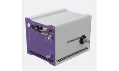
Manufactured by:Atonarp Inc. based inMinato-Ku, JAPAN
Its customizable proprietary software puts precision molecular analysis for Lyophilization, industrial process control and select semiconductor applications at your ...
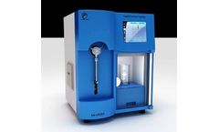
Manufactured by:Sterilbio Analytics Pte. Ltd. based inSingapore, SINGAPORE
The Sterilbio Analytics Model SA-LPC07 Liquid Particle Counter is designed to accurately measure suspended particles in a range of environments, particularly suitable for Water for Injection, Medical Device Cleaning, Precision Parts Cleaning, and Semiconductor Waters. Utilizing the Light Obscuration Principle, this device ensures compliance with USP, BP, and CHP standards. The ...
by:Theramx Inc. based inSeongnam-si, SOUTH KOREA
Biosensing technology that enables early diagnosis and prevention of diseases through an analysis of complex causal substances (proteins, lipids, organic acids, etc.) for dementia or metabolic syndrome, etc., as well as analysis/detection of composite biomarkers utilizing AI technology. ...
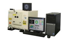
Manufactured by:Nidek Co., Ltd. based inAichi, JAPAN
The measured data can be quickly acquired by full surface analysis with laser light. The measurement result can be displayed as measured values, contour map, bird's-eye view, cross-section view, etc. Original phase shift method is applicable to multiple interference fringes System control with exclusive analyzer running on the Windows platform provides easy operation. Transparent samples can not ...
Premium
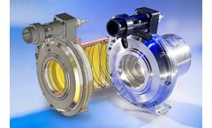
Manufactured by:Zygo Corporation - AMETEK, Inc based inMiddlefield, CONNECTICUT (USA)
Lasers continue to be employed in an ever widening application space. One of the most common challenges is getting the laser from the source to the object, with the right power, size and shape. We develop laser beam delivery systems that employ CW or pulsed pico-/femto- second lasers in the UV-to-IR across a wide range of applications ...
Manufactured by:Sixtus Italia srl based inPrato, ITALY
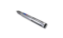
Technical Specification: Laser Type: semiconductor laser. Class: IV (complying with IEC 60825-1). Classification: II b ...
Manufactured by:Asetronics AG based inBern, SWITZERLAND
Working together with OSRAM Opto Semiconductors the successor product was developed on the proven basis of the predecessor LED, and new and exclusively produced and sold by ...
Manufactured by:CardiacSense based inCaesarea, ISRAEL
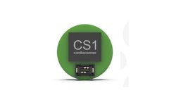
CardiacSense’s disruptive technology allows it to turn out medical-grade products. We signed an MOU (Memorandum of Understanding) with a leading semiconductor manufacturer for designing and manufacturing a SOM (System on ...
Manufactured by:Exogenesis Corporation based inBillerica, MASSACHUSETTS (USA)
NanoAccell is used for ultra-shallow processing of surfaces used for biomedical applications, for optical components, for semiconductor devices, and for other nanosurface modified products. In ANAB, a beam of accelerated gas cluster ions is initially produced as described in GCIB, but the gas cluster is caused to dissociate and a deflector removes the ...
Manufactured by:Nanjing Binzhenghong Instrument Co., Ltd based inQixia District, CHINA
Good chemical resistance, can withstand most chemical solvents (strong acid, strong alkali, aqua regia and various organic solvents); As a high-quality, high-performance new material carrier, PTFE silicon wafer carrier is widely used in various fields, such as semiconductor manufacturing, electronics industry, medical treatment, etc. Its special structure gives it good ...
Manufactured by:Jenoptik AG based inJena, GERMANY
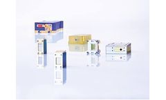
Jenoptik develops and produces high-power diode lasers – ranging from semiconductor material, Mounted Diode Lasers and laser stacks to fiber-coupled diode laser modules. We thereby cover the entire process and technology chain for laser material processing. Our diode lasers have been well-established as high-quality machine tools in industry, medicine and science for many ...
Manufactured by:Radiation Detection Technologies, Inc. (RDT) based inManhattan, KANSAS (USA)
CdTe and CdTe hybrid single crystal devices have recently shown promise for high count rate medical imaging applications. The high spatial resolution of these semiconductor materials, compared to that of scintillators, offers superior efficiency and image quality in the most advanced medical imaging instruments. Recent developments with the Accelerated Crucible Rotation Technique ...
Manufactured by:Nanjing Binzhenghong Instrument Co., Ltd based inQixia District, CHINA
Technical parameters Product name: PFA reagent bottle Specifications (ml): 30/ 50/ 60/ 100/ 125/ 250/ 300/ 500/ 1000/ 2000/ 3000/ 4000/ 5000 Material: PFA Temperature tolerance: -196-260 degrees Celsius PFA sample bottles are used for semiconductors, new materials, new energy, geochemistry, trace element detection, and ICP-MS analysis experiments because of their excellent ...
Manufactured by:H&abyz Co., Ltd. based inYongin-si, SOUTH KOREA
H&abyz Model HAD1717MC Flat Panel Detector(DR system) Features: · Detector technology: Cesium Iodide (CsI:Tl) Scintillator with Material Amorphous Silicon (a-Si) TFT semiconductor · Type of communication: Wired(Tethered) · Pixel Pitch: 140 µm · Spatial resolution: 3.57 lp/mm · Exterior dimensions 460*460*15 mm (17*17"") · Matrix size: 3052*3052 pixels · Weight: 3.75 kg · ...
Manufactured by:PTW Freiburg GmbH based inFreiburg, GERMANY
Field-class electrometer acc. to IEC 60731 for air kerma measurements in radiotherapy and orthovoltage therapy. Outstanding accuracy (± 2%) and excellent resolution (20 fA). Connection of semiconductor detectors or ion chambers or of the NOMEX® Multimeter. Combined with the NOMEX Multimeter and/or NOMEX mAs all relevant QC parameters can be captured in one single ...
Manufactured by:3P Performance Plastics Products based inFRANCE
Its renowned chemical resilience and electrical properties facilitate its usage in demanding sectors like the semiconductor and pharmaceutical industries. The minimal contamination level during its production further enhances its preference in such sectors. ...
Manufactured by:APT Advanced Polymer Tubing GmbH based inDüsseldorf-Benrath, GERMANY
Additionally, APT can produce these tubes using FDA-compliant raw materials for applications within the food and beverage industry. The company is recognized for its high-purity tubing solutions, notably certified for the semiconductor sector. Moreover, APT's tubing products meet the stringent standards of NSF certification for food contact, and the quality is further affirmed by ...
Manufactured by:Erba Mannheim based inLondon, UNITED KINGDOM
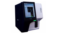
Intensity of light scattered from semiconductor laser beam on the blood cells reflects cell size and intra cellular density. Low angle scatter shows cell size, while the middle and high angle display intracellular information (nucleus and cytoplasmic content). Pulse data thus captured plots 4 2D scattergrams. ...
Manufactured by:Schneider-Kreuznach based inBad Kreuznach, GERMANY
These filters are particularly adept at revealing hidden details not visible to the naked eye, such as moisture in materials, defects in semiconductors, or underlying layers in artwork. Schneider-Kreuznach's SWIR filters feature narrow bandwidth and steep edges, allowing for precise detection and improved quality of analyses. They are used extensively in spectroscopy for chemical ...

