Industrial Vision Technology (S) Pte Ltd
- Home
- Companies
- Industrial Vision Technology (S) Pte ...
- Products
- Wafer Defect Inspection System
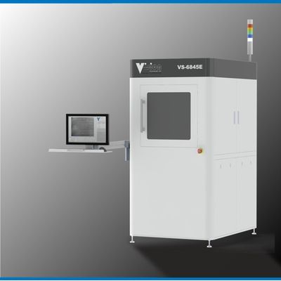
Wafer Defect Inspection System
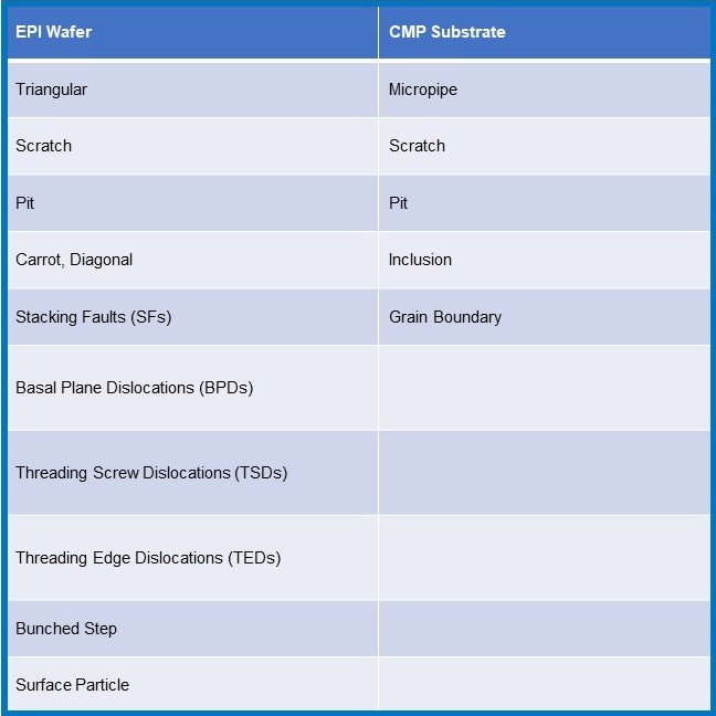
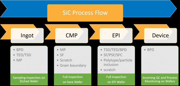
Comply with IEC63068-3 Standard: Test method for defects using photoluminescence, Model VS-6845 SiC Wafer defect inspection system has capability on Non-destructive recognition criteria of defects in silicon carbide homoepitaxial wafer for power devices.
Most popular related searches
wafer defect inspection system
wafer defect inspection
defect inspection system
wafer defect
inspection system
wafer inspection system
non-destructive inspection
wafer inspection
surface inspection
process control system
The system uses near ultraviolet photoluminescence (NUV-PL) technology to perform high-speed, high-sensitivity and non-destructive inspection for crystal defects which cannot be detected with conventional visible light surface inspection
High Sensitivity to defects on SiC Substrate and 4H-SiC Epitaxy wafer, especially yield-impacting defects, enabling enhanced quality control and fast root cause determination, to improve MOCVD process control.
The system accelerated deep learning with GPU and Artificial Intelligent software to classify the defect more accurately.
Our AI_DL Auto Classification software can run in offline and easy to use.